- PCB manufacturing capability
- PCB manufacturing equipment
Introducing our high-quality RF Printed Circuit Boards (PCBs) — the perfect solution for all your radio frequency (RF) circuitry needs. These cutting-edge PCBs are meticulously designed and manufactured to ensure optimal performance, and also efficiency in a wide range of RF applications.
Whether you’re working on wireless communication systems, or any other RF-based project, our RF PCBs are built to meet and exceed your expectations.
Invest in our RF Printed Circuit Boards and unlock the full potential of your RF-based projects. With their exceptional RF performance, design flexibility, and reliability, our RF PCBs are the ideal choice for engineers, researchers, and industry professionals.
Advantages of RF Printed Circuit Boards:
- Enhanced RF Performance: Our RF PCBs are engineered to deliver exceptional signal integrity, low loss, and minimal noise interference. They also offer superior impedance control and excellent high-frequency characteristics.
- Advanced Material Selection: We utilize premium-grade materials with excellent dielectric properties, such as high-frequency laminates to ensure superior RF performance. These materials minimize signal loss, crosstalk, and phase distortion. It also results in improved overall system performance.
- Design Flexibility: Our RF PCBs are available in various configurations, including single-sided, double-sided, and multi-layered options. They can be customized to meet your specific requirements, accommodating complex RF circuit designs and component placement while optimizing signal integrity.
- Reliable Manufacturing: We employ state-of-the-art manufacturing processes and adhere to stringent quality control measures to ensure consistent production of reliable. Our manufacturing facilities are equipped with advanced machinery and skilled technicians. It also ensures a precision and accuracy at every step of the production process.
- Thorough Testing: Each RF PCB undergoes rigorous testing and inspection to guarantee its compliance with industry standards and specifications. We conduct comprehensive RF testing, impedance matching analysis, and quality checks to ensure that our PCBs meet the highest performance standards.
| Standard PCB Production Capability | |
| Feature | Capability |
| Quality Grade | Standard IPC 2 |
| Number of Layers | 1 – 32layers |
| Order Quantity | 1pcs – 10,000,000 pcs |
| Build Time | 2days – 5weeks (Expedited Service) |
| Material | FR-4 Standard Tg 150°C, FR4-High Tg 170°C, FR4-High-Tg 180°C, FR4-Halogen-free, FR4-Halogen-free & High-Tg |
| Board Size | Min 6*6mm | Max 600*700mm |
| Board size tolerance | ±0.1mm – ±0.3mm |
| Board Thickness | 0.4mm – 3.2mm |
| Board Thickness Tolerance | ±0.1mm – ±10% |
| Copper Weight | 0.5oz – 6.0oz |
| Inner Layer Copper Weight | 0.5oz – 2.0oz |
| Copper Thickness Tolerance | +0μm +20μm |
| Min Tracing/Spacing | 3mil/3mil |
| Solder Mask Sides | As per the file |
| Solder Mask Color | Green, White, Blue, Black, Red, Yellow |
| Silkscreen Sides | As per the file |
| Silkscreen Color | White, Blue, Black, Red, Yellow |
| Surface Finish | HASL – Hot Air Solder Leveling |
| Lead Free HASL – RoHS | |
| ENIG – Electroless Nickle/Immersion Gold – RoHS | |
| ENEPIG – Electroless Nickel Electroless Palladium Immersion Gold – RoHS | |
| Immersion Silver – RoHS | |
| Immersion Tin – RoHS | |
| OSP -Organic Solderability Preservatives – RoHS | |
| Min Annular Ring | 3mil |
| Min Drilling Hole Diameter | 6mil, 4mil-laser drill |
| Min Width of Cutout (NPTH) | 0.8mm |
| NPTH Hole Size Tolerance | ±.002″ (±0.05mm) |
| Min Width of Slot Hole (PTH) | 0.6mm |
| PTH Hole Size Tolerance | ±.003″ (±0.08mm) – ±4mil |
| Surface/Hole Plating Thickness | 20μm – 30μm |
| SM Tolerance (LPI) | .003″ (0.075mm) |
| Aspect Ratio | 1.10 (hole size: board thickness) |
| Test | 10V – 250V, flying probe or testing fixture |
| Impedance tolerance | ±5% – ±10% |
| SMD Pitch | 0.2mm(8mil) |
| BGA Pitch | 0.2mm(8mil) |
| Chamfer of Gold Fingers | 20, 30, 45, 60 |
| Other Techniques | Gold fingers |
| Blind and Buried Holes | |
| peelable solder mask | |
| Edge plating | |
| Carbon Mask | |
| Kapton tape | |
| Countersink/counterbore hole | |
| Half-cut/Castellated hole | |
| Press fit hole | |
| Via tented/covered with resin | |
| Via plugged/filled with resin | |
| Via in pad | |
| Electrical Test | |
PCB Drilling machine
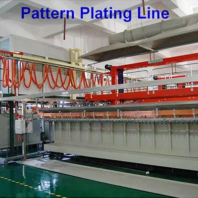
PCB pattern plating line
PCB solder mask expose machine
PCB pattern expose machine
Strip film etching line
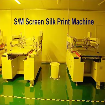
Solder mask screen silk print machine
Solder mask scrubbing line
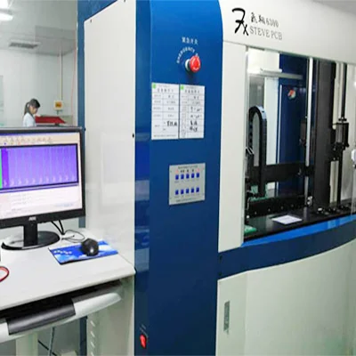
PCB Flying Probe Test (FPT)
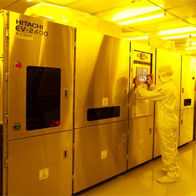
Fully automatic exposure machine


