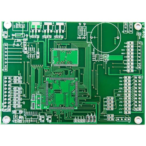
Прототип материнской платы вытяжки
Название: печатная плата материнской платы вытяжки
Пластина: KB6165G
Толщина пластины: 1,6 мм
Слои: 2л
Размер: 82,63*46,7 мм
Минимальная апертура: 0,296 мм
Ширина линии/момент: 0,342*0,37 мм
Толщина медной фольги: 1/1 унции
Обработка поверхности: процесс золотого покрытия
Паяльная маска/персонаж: черное масло и белые символы.
Печатная плата прибора для завивки волос
Название: монтажная плата для завивки волос
Лист: ФР-4
Толщина пластины: 1,0 мм
Слои: 2л
Размер: 76,82*13,6 мм
Минимальная апертура: 0,32 мм
Ширина линии/момент: 0,3*0,41 мм
Толщина медной фольги: 1/1 унции
Обработка поверхности: Антиоксидант OSP
Паяльная маска/персонаж: черное масло и белые символы.
Прототип печатной платы для сигнализации электромобиля
Название: печатная плата сигнализации электромобиля
Пластина: KB6165F
Толщина пластины: 1,6 мм
Слои: Двусторонний
Размер: 67*41,37 мм
Минимальная апертура: 0,33 мм
Ширина линии/момент: 0,36*0,44 мм
Толщина медной фольги: 35 мкм
Обработка поверхности: бессвинцовый аэрозольный баллончик.
Паяльная маска/символ: зеленый масляный белый символ
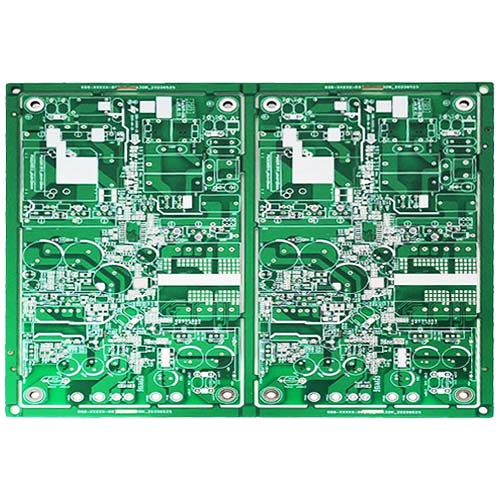
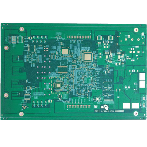
Прототип печатной платы питания сервера
Название: Плата питания сервера
Пластина: KB6167F
Толщина пластины: 1,6 мм
Слои: 2л
Размер: 78,26*61,3 мм
Минимальная апертура: 0,281 мм
Ширина линии/момент: 0,21*0,186 мм
Толщина медной фольги: 1/1 унции
Обработка поверхности: бессвинцовый аэрозольный баллончик.
Паяльная маска/символ: зеленый масляный белый символ
Прототип печатной платы динамика электрогитары
Название: печатная плата динамика электрогитары
Лист: ФР-4
Толщина пластины: 1,0 мм
Слои: 2л
Размер: 86,9*73,58 мм
Минимальная апертура: 0,236 мм
Ширина линии/момент: 0,32*0,37 мм
Толщина медной фольги: 1/1 унции
Обработка поверхности: бессвинцовый аэрозольный баллончик.
Паяльная маска/символ: зеленый масляный белый символ
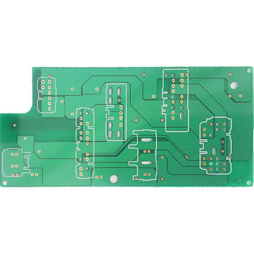
Двусторонние печатные платы со сквозными отверстиями
Название: Двусторонние печатные платы со сквозными отверстиями
Лист: ФР-4
Толщина пластины: 1,0 мм
Слои: 2л
Размер: 86,9*73,58 мм
Минимальная апертура: 0,236 мм
Ширина линии/момент: 0,32*0,37 мм
Толщина медной фольги: 1/1 унции
Обработка поверхности: бессвинцовый аэрозольный баллончик.
Паяльная маска/символ: зеленый масляный белый символ
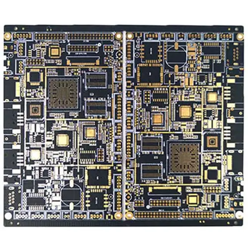
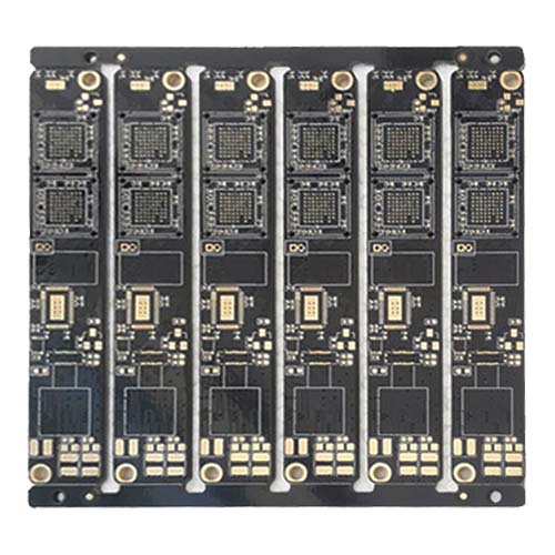
- PCB Prototype Capability
- PCB manufacturing equipment
Introducing our PCB Prototype, a cutting-edge solution for rapid prototyping and development of electronic circuits. Our PCB Prototype seamlessly integrates with popular design software, making it convenient to transfer your circuit schematics and layout files.
Our dedicated team of experts is ready to assist you throughout the PCB prototyping process. Whether you have technical questions, need design guidance, or require assistance with your order, our knowledgeable support staff is here to help.
Experience the power of our PCB and accelerate your product development journey. From concept to reality, we’re here to provide you with high-quality, fast, and also customizable PCB prototypes that meet your exact specifications.
Advantages of PCB Prototype:
- High-Quality Manufacturing: Our PCB is fabricated using state-of-the-art manufacturing processes and materials. We employ advanced techniques to ensure exceptional quality and reliability in every circuit board produced.
- Quick Turnaround Time: We understand the importance of speed in the product development cycle. With our PCB Prototype, you can expect fast turnaround times. This also allows you to iterate and test your designs quickly. Reduce your time to market and gain a competitive edge.
- Customization Options: Our PCB supports a wide range of customization options to cater to your specific needs. From choosing different board sizes and shapes to selecting the number of layers and solder mask colors, we provide flexibility to tailor the prototype to your requirements.
- High Precision: We utilize cutting-edge equipment and follow stringent quality control processes to achieve high precision in our PCB prototypes. Every component pad, trace, and drill hole is meticulously crafted to ensure accurate and reliable connections, giving you confidence in your designs.
- Compatibility: Our PCB supports compatibility with various electronic components, including through-hole and surface mount devices (SMDs). This versatility also allows you to seamlessly integrate different types of components into your prototypes.
| PCB Prototype Features | Capability |
| Quality Grade | Standard IPC 1-3 |
| Number of Layers | 1 – 32layers |
| Order Quantity | 1pcs + |
| Build Time | 2 – 15 days |
| Material | Rigid: FR2, CEM-1, CEM-3, FR4 (standard – halogen-free – high performance) including ShengYi, Iteq, Elite Materials Corp., NanYa, Kingboard, Grace, TUC, Meteorwave |
| Flex: PI, PET Including Taiflex, Dupont FR & AP, Panasonic, ShengYi, Doosan. Hanwha, SF305 | |
| Metal Core: Metal Core Aluminum based material Including Bergquist MP, HT & CML, ITEQ T-Lam, Laird TLAM SS Taiflex, Dupont FR & AP, Panasonic, ShengYi, Doosan. Arlon,Ventec and suggested local material brand( for detail pls contact our sales) | |
| Board Size | Maximum 610mm*1200mm (24” * 47″”) |
| Board Thickness | Rigid PCB : 0.15mm – 10 mm |
| FLEX PCB: 0.05mm – 0.16mm | |
| Board Thickness tolerance | / |
| Copper Weight | 1.0oz – 15.0oz |
| Inner Layer Copper Weight | 0.5oz – 12.0oz |
| Min Trace/Space( track/gap or width/space) | 2mil/2mil (0.05mm/0.05mm) |
| Solder Mask Color | Green, White, Blue, Black, Red, Yellow or others |
| Silkscreen Color | White, Black or others |
| Surface Finish | ENIG / GF / OSP / I Ag / HASL (lead) / HASL (Leadfree) / Plating Au/Ni/ Immersion Sn / GF+OSP / GF+HASL / OSP+ENIG /IAG+GF/Isn+GF |
| Min Annular Ring | 5mil |
| Min Drilling Hole Diameter | mechanical: 0.1mm |
| laser : 0.05mm | |
| NPTH Hole Size Tolerance | ±0.025mm |
| PTH Hole Size Tolerance | ±.003″ (±0.08mm) – ±.006″ (±0.15mm) |
| Surface/Hole Plating Thickness | 20μm – 30μm |
| SM Tolerance (LPI) | .003″ (0.075mm) |
| Aspect Ratio | 20:1 (board thickness: hole size) |
| Test | 10V – 250V, flying probe or testing fixture |

PCB Drilling machine

PCB pattern plating line

PCB solder mask expose machine

PCB pattern expose machine

Strip film etching line

Solder mask screen silk print machine

Solder mask scrubbing line

PCB Flying Probe Test (FPT)

Fully automatic exposure machine

we provide 24-hour service and support, you will receive a reply to your question within 2 hours and a quotation within 24 hours.

Own PCB factory of 50,000 square meters, the monthly output can reach 60,000 square meters, no minimum PCB order requirements

Before the official production of the PCB, we will conduct a free DFM review service and support free Allegro, Altium, Protel, PADS, OBD, Gerber and other formats.

We can provide you with high frequency, high TG, high CTI, buried blind via, aluminum based PCB manufacturing, the quality is fully compliant with IPC 610-D standard, testing and quality assurance
We provide Cooker hood mother board PCB services. Leadsintec is your one stop turnkey PCB assembly fac...
Leadsintec provides hair curler PCB circuit board services. This is a PCBA one-stop assembly factory w...
We are a professional PCBA one-stop assembly factory, Leadsintec supports Electric vehicle alarm PCB P...
We support Server Power Backplane PCB business, Leadsintec is a professional one-stop PCBA service fact...
Leadsintec supports Electric guitar speaker PCB business, we are a professional PCBA one-stop assembly...
We provide Double-sided through-hole PCB boards services. Leadsintec is your one stop turnkey PCB asse...