Монтажная плата светодиодного освещения
Название: Сборка монтажной платы светодиодного освещения для электроники
Происхождение: Китай
Сертифицировано: UL, CE, RoHS.
Слой: 1, 2, 4, 6, до 24 слоев.
Материал: FR-4, High Tg, Isola, алюминий, Rogers и т. д.
Толщина платы: по индивидуальному заказу
Цвет паяльной маски: обычно белый, в эстетических целях.
Поверхностная обработка: HASL/бессвинцовый HASL

Конструкция сборки печатной платы наружного фонаря
Название: Конструкция сборки печатной платы СИД для наружного использования – Светящиеся фонари
Происхождение: Китай
Сертифицировано: UL, CE, RoHS.
Материал: медь
Применение: для наружного освещения
Толщина платы: по индивидуальному заказу
Цвет паяльной маски: обычно белый, в эстетических целях.
Поверхностная обработка: HASL/бессвинцовый HASL

Производитель печатных плат для внутренних фонарей – PCBA/PCB
Название: Производитель печатных плат для внутренних фонарей – PCBA/PCB
Происхождение: Китай
Сертифицировано: UL, CE, RoHS.
Материал: медь
Применение: для освещения
Толщина платы: по индивидуальному заказу
Цвет паяльной маски: обычно белый, в эстетических целях.
Поверхностная обработка: HASL/бессвинцовый HASL

Проектирование сборки автомобильной светодиодной печатной платы
Название: Проектирование сборки автомобильной светодиодной печатной платы
Происхождение: Китай
Сертифицировано: UL, CE, RoHS.
Материал: стекловолокно, эпоксидная смола+ полиимидная смола.
Применение: для легковых и грузовых автомобилей, узлов.
Толщина платы: по индивидуальному заказу
Количество слоев печатной платы: 4-40 (многослойные)
Цвет паяльной маски: обычно белый, в эстетических целях.
Поверхностная обработка: HASL/бессвинцовый HASL

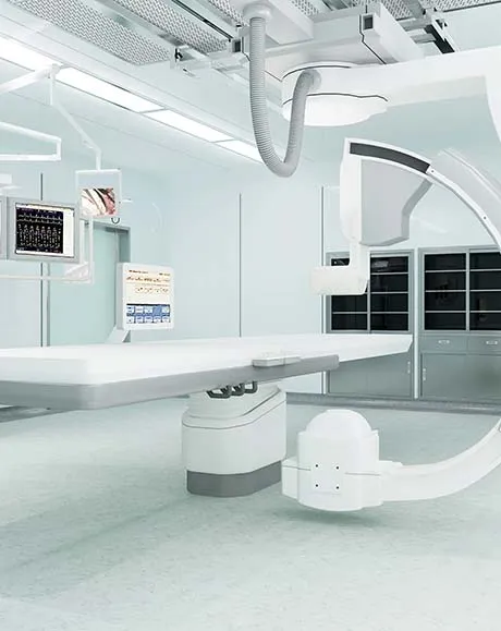
Сборка печатной платы медицинского светодиода
Название: Медицинская светодиодная печатная плата в сборе
Происхождение: Китай
Сертифицировано: UL,CE, ROHS,
Толщина платы: по индивидуальному заказу
Поверхностная обработка: HASL/бессвинцовый HASL
Цвет паяльной маски: типичный белый, для эстетических целей.
применение: свет

Сборка печатной платы светодиодной ленты
Название: Сборка печатной платы светодиодной ленты
происхождение: Китай
Толщина платы: Индивидуальные
Цвет паяльной маски: Обычно белый, для эстетических целей.
Поверхностная обработка: HASL \ HASL без свинца
Применения: Свет
- PCB Assembly Capability
- PCB Assembly Equipment
LED PCB Assembly is a specialized electronic manufacturing service that focuses on the assembly of printed circuit boards (PCBs) specifically designed for LED (Light Emitting Diode) applications. It involves the precise placement and soldering of LED components onto the PCB to create functional LED lighting modules or systems.
LED PCB Assembly is tailored to meet the unique requirements of LED technology. This also ensures the efficient and reliable operation of LED lighting products. It incorporates design considerations, thermal management techniques, and high-quality components to optimize the performance, longevity, and energy efficiency of LED-based lighting solutions.
Advantages of LED PCB Assembly:
- Optimal Thermal Management: LED PCB Assembly considers the thermal management requirements of LEDs to ensure optimal heat dissipation. The PCB design incorporates heat sinks, thermal vias, and copper traces to efficiently transfer heat away from the LED components, maximizing their lifespan and maintaining their performance over time.
- Precision LED Placement: LED PCB also utilizes automated pick-and-place machines to accurately position and align LED components on the PCB. This precision placement ensures consistent light output, color uniformity, and visual aesthetics in LED lighting products.
- Efficient Power Distribution: LED PCB incorporates power distribution circuitry to deliver regulated and stable power to the LED components. This also ensures uniform brightness, minimizes flickering, and optimizes the energy efficiency of the LED lighting system.
- Customized LED Configuration: LED Assembly allows for customized LED configurations to meet specific lighting requirements. This includes variations in LED types (such as SMD or through-hole), color combinations (RGB, single-color, or multi-color), and intensity levels. This also enables flexibility in creating various lighting effects and designs.
- PCB Design Optimization: LED PCB focuses on optimizing the PCB layout and traces to minimize signal losses and maximize the electrical performance of the LED lighting system. Considerations such as proper grounding, signal integrity, and noise immunity are taken into account to ensure reliable and consistent operation.
| SMT capacity: 19 million points/day | ||
| Testing Equipment | X-RAY Nondestructive Tester, First Piece Tester, AOI Automatic Optical Tester, ICT Tester, BGA Rework Station | |
| Placement speed | Chip placement speed (at best conditions) 0.036 S/piece | |
| Mounted Component Specifications | Pasteable smallest package | |
| Minimum device accuracy | ||
| IC type chip accuracy | ||
| Mounted PCB Specifications | Substrate size | |
| Substrate thickness | ||
| throw rate | 1. Resistance-capacitance ratio 0.3% | |
| 2. IC type without throwing material | ||
| Board Type | POP/common board/FPC/rigid-flex board/metal substrate | |
| DIP daily production capacity | ||
| DIP plug-in production line | 50000 points/day | |
| DIP post welding production line | 20000 points/day | |
| DIP test production line | 50000pcs PCBA/day | |
| Assembly processing capability | ||
| The company has more than 10 advanced assembly production lines, dust-free and anti-static air-conditioning workshop, TP dust-free workshop, equipped with aging room, test room, functional test isolation room, advanced and perfect equipment, can carry out various product assembly, packaging, testing, Aging, etc. production. Monthly production capacity can reach 150,000 to 300,000 sets/month | ||
| PCBA processing capability | ||
| project | Mass processing capability | Small batch processing capability |
| Number of layers (max) | 2-18 | 20-30 |
| Plate type | FR-4, Ceramic Sheet, Aluminum Base Sheet PTFE, Halogen Free Sheet, High Tg Sheet | PTFE, PPO, PPE |
| Rogers,etc Teflon | E-65, ect | |
| Sheet mixing | 4 layers – 6 layers | 6th floor – 8th floor |
| biggest size | 610mm X 1100mm | / |
| Dimensional Accuracy | ±0.13mm | ±0.10mm |
| Plate thickness range | 0.2mm–6.00mm | 0.2mm–8.00mm |
| Thickness tolerance ( t≥0.8mm) | ±8% | ±5% |
| Thickness tolerance (t<0.8mm) | ±10% | ±8% |
| Media thickness | 0.076mm–6.00mm | 0.076mm–0.100mm |
| Minimum line width | 0.10mm | 0.075mm |
| Minimum spacing | 0.10mm | 0.075mm |
| Outer copper thickness | 8.75um–175um | 8.75um–280um |
| Inner layer copper thickness | 17.5um–175um | 0.15mm–0.25mm |
| Drilling hole diameter (mechanical drill) | 0.25mm–6.00mm | 0.15mm–0.25mm |
| Hole diameter (mechanical drill) | 0.20mm–6.00mm | 0.10mm–0.20mm |
| Hole Tolerance (Mechanical Drill) | 0.05mm | / |
| Hole tolerance (mechanical drill) | 0.075mm | 0.050mm |
| Laser Drilling Aperture | 0.10mm | 0.075mm |
| Plate thickness aperture ratio | 10:1 | 12:1 |
| Solder mask type | Photosensitive green, yellow, black, purple, blue, ink | / |
| Minimum Solder Mask Bridge Width | 0.10mm | 0.075mm |
| Minimum Solder Mask Isolation Ring | 0.05mm | 0.025mm |
| Plug hole diameter | 0.25mm–0.60mm | 0.60mm-0.80mm |
| Impedance tolerance | ±10% | ±5% |
| Surface treatment type | Hot air leveling, chemical nickel gold, immersion silver, electroplated nickel gold, chemical immersion tin, gold finger card board | Immersion Tin, OSP |

Automatic Solder Paste Printing Machine

AOI Optical Inspection

Smt High-Speed Placement Machine

Nitrogen Reflow Soldering

X-Ray

Three Anti-Paint Spraying Machine

SPI Solder Paste Thickness Tester

Automatic Wave Soldering Machine

First Article Inspection
Our complete turnkey PCB assembly service provides a 24 hour quote service for your turnkey PCB assembly order.
Leadsintec cooperates with world-renowned component suppliers to ensure that the source of electronic components is plastic and the authenticity is guaranteed.
It has 7 fully automatic SMT high-speed chip production lines, equipped with ten temperature zone nitrogen reflow ovens, online AOI, SPI, X-RAY and other equipment.
We have complete ISO9001, ISO13485, ISO14001, IATF 16949, UL and other system certifications, and our products meet environmental protection requirements.