PCB и PCBA Плата солнечного гибридного инвертора
Название: PCB & PCBA Плата солнечного гибридного инвертора
Происхождение: Китай
Сертифицировано: UL, CE, RoHS.
Цвет паяльной маски: синий. зеленый. красный. черный. белый. и т. д.
Слой: 1-24 слоя
Поверхностная обработка: HASL\OSP\погружное золото
Толщина меди: 1 унция
Базовый материал: FR-4/алюминий/керамика/cem-3/FR-1

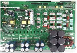
Гибридный солнечный инвертор на печатной плате мощностью 5 кВт в сборе
Имя: Сборка печатной платы солнечного инвертора на 5 кВт
Происхождение: Китай
Сертифицировано: UL, CE, RoHS.
Поверхностная обработка: OSP, HASL, иммерсионное золото, иммерсионное олово и т. д.
Толщина платы: по индивидуальному заказу
Паяльная маска: зеленая, черная, синяя, красная, белая и т. д.
Толщина меди: 1 унция, 2 унции, 3 унции, 4 унции, 5 унций

Гибридная сборка печатной платы FR4 + RO4350B
Название: Гибридная печатная плата в сборе FR4 + RO4350B
Происхождение: Китай
Сертифицировано: UL, CE, RoHS.
Поверхностная обработка: OSP, HASL, иммерсионное золото, иммерсионное олово и т. д.
Толщина платы: по индивидуальному заказу
Толщина меди: 1 унция, 2 унции, 3 унции, 4 унции, 5 унций
Паяльная маска: зеленая, черная, синяя, красная, белая и т. д.

Гибридная печатная плата солнечного инвертора мощностью 5 кВт в сборе
Название: Гибридная плата солнечного инвертора 5 кВт в сборе
Происхождение: Китай
Сертифицировано: UL, CE, RoHS.
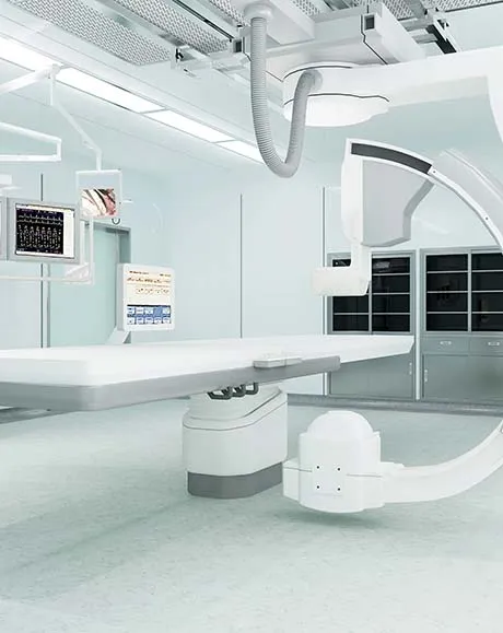
Применение: Световой инвертор
Поверхностная обработка: HASL/бессвинцовый HASL
Паяльная маска: зеленая, синяя, белая, красная и т. д.

PCB и PCBA Плата солнечного гибридного инвертора
Название: PCB & PCBA Плата солнечного гибридного инвертора
Происхождение: Китай
Сертифицировано: UL, CE, RoHS.
Толщина меди: 1 унция
Базовый материал: FR-4/алюминий/керамика/cem-3/FR-1
Применение: Электронное устройство
Толщина платы: по индивидуальному заказу

PCB плата гибридного солнечного инвертора
Название: Плата печатной платы солнечного гибридного инвертора
Происхождение: Китай
Сертифицировано: UL, CE, RoHS.
Материал: FR4, с высоким ТГ, безгалогеновый, высокочастотный.
Обработка поверхности: HASL/погружное золото/погружное серебро/погружное олово
Маска для пайки печатной платы: белый, черный, желтый, зеленый, красный, синий
Применение: Бытовая электроника/Бытовая техника/Медицинское оборудование
- PCB Assembly Capability
- PCB Assembly Equipment
Hybrid PCB Assembly is an advanced electronic manufacturing process that involves the integration of different technologies and components onto a single printed circuit board (PCB). It combines both surface mount technology (SMT) and through-hole technology (THT) assembly methods. It also allows for the incorporation of diverse components and functionalities.
Hybrid PCB Assembly offers the flexibility to combine the benefits of SMT, which enables high component density and compactness, with THT, which provides robust mechanical connections and higher power handling capabilities. This combination makes it ideal for applications where a mix of components with varying requirements is needed.
The assembly process for Hybrid PCBs involves the placement and soldering of SMT components on one side of the PCB, while THT components are inserted through pre-drilled holes on the opposite side and soldered manually or with wave soldering techniques. The combination of SMT and THT allows for a wider range of components. It includes ICs, resistors, capacitors, connectors, transformers, and more.
Advantages of Hybrid PCB Assembly:
- Component Flexibility: Hybrid Assembly offers the flexibility to incorporate a wide range of components, including both SMT and THT components. This allows for the integration of components with different form factors, power ratings, and specialized functionalities on a single PCB, making it suitable for diverse application requirements.
- Design Versatility: Hybrid Assembly provides design versatility, enabling engineers to optimize the layout and functionality of the PCB. The combination of SMT and THT technologies allows for greater flexibility in component placement, routing, and thermal management. This also results in improved overall design efficiency.
- Higher Component Density: By utilizing SMT technology, Hybrid Assembly enables higher component density compared to traditional THT-only assemblies. This allows for compact PCB designs, which are particularly beneficial in space-constrained applications.
- Mechanical Stability: THT components, with their leads passing through pre-drilled holes and soldered on the opposite side of the PCB, provide enhanced mechanical stability and durability. This makes Hybrid PCBs suitable for applications that require robust connections, resistance to mechanical stress, or exposure to vibrations.
- Power Handling Capabilities: THT components can handle higher power levels compared to their SMT counterparts. By incorporating THT components in a Hybrid Assembly, it becomes possible to accommodate higher power requirements, such as power amplifiers, transformers, or high-current connectors.
| SMT capacity: 19 million points/day | ||
| Testing Equipment | X-RAY Nondestructive Tester, First Piece Tester, AOI Automatic Optical Tester, ICT Tester, BGA Rework Station | |
| Placement speed | Chip placement speed (at best conditions) 0.036 S/piece | |
| Mounted Component Specifications | Pasteable smallest package | |
| Minimum device accuracy | ||
| IC type chip accuracy | ||
| Mounted PCB Specifications | Substrate size | |
| Substrate thickness | ||
| throw rate | 1. Resistance-capacitance ratio 0.3% | |
| 2. IC type without throwing material | ||
| Board Type | POP/common board/FPC/rigid-flex board/metal substrate | |
| DIP daily production capacity | ||
| DIP plug-in production line | 50000 points/day | |
| DIP post welding production line | 20000 points/day | |
| DIP test production line | 50000pcs PCBA/day | |
| Assembly processing capability | ||
| The company has more than 10 advanced assembly production lines, dust-free and anti-static air-conditioning workshop, TP dust-free workshop, equipped with aging room, test room, functional test isolation room, advanced and perfect equipment, can carry out various product assembly, packaging, testing, Aging, etc. production. Monthly production capacity can reach 150,000 to 300,000 sets/month | ||
| PCBA processing capability | ||
| project | Mass processing capability | Small batch processing capability |
| Number of layers (max) | 2-18 | 20-30 |
| Plate type | FR-4, Ceramic Sheet, Aluminum Base Sheet PTFE, Halogen Free Sheet, High Tg Sheet | PTFE, PPO, PPE |
| Rogers,etc Teflon | E-65, ect | |
| Sheet mixing | 4 layers – 6 layers | 6th floor – 8th floor |
| biggest size | 610mm X 1100mm | / |
| Dimensional Accuracy | ±0.13mm | ±0.10mm |
| Plate thickness range | 0.2mm–6.00mm | 0.2mm–8.00mm |
| Thickness tolerance ( t≥0.8mm) | ±8% | ±5% |
| Thickness tolerance (t<0.8mm) | ±10% | ±8% |
| Media thickness | 0.076mm–6.00mm | 0.076mm–0.100mm |
| Minimum line width | 0.10mm | 0.075mm |
| Minimum spacing | 0.10mm | 0.075mm |
| Outer copper thickness | 8.75um–175um | 8.75um–280um |
| Inner layer copper thickness | 17.5um–175um | 0.15mm–0.25mm |
| Drilling hole diameter (mechanical drill) | 0.25mm–6.00mm | 0.15mm–0.25mm |
| Hole diameter (mechanical drill) | 0.20mm–6.00mm | 0.10mm–0.20mm |
| Hole Tolerance (Mechanical Drill) | 0.05mm | / |
| Hole tolerance (mechanical drill) | 0.075mm | 0.050mm |
| Laser Drilling Aperture | 0.10mm | 0.075mm |
| Plate thickness aperture ratio | 10:1 | 12:1 |
| Solder mask type | Photosensitive green, yellow, black, purple, blue, ink | / |
| Minimum Solder Mask Bridge Width | 0.10mm | 0.075mm |
| Minimum Solder Mask Isolation Ring | 0.05mm | 0.025mm |
| Plug hole diameter | 0.25mm–0.60mm | 0.60mm-0.80mm |
| Impedance tolerance | ±10% | ±5% |
| Surface treatment type | Hot air leveling, chemical nickel gold, immersion silver, electroplated nickel gold, chemical immersion tin, gold finger card board | Immersion Tin, OSP |

Automatic Solder Paste Printing Machine

AOI Optical Inspection

Smt High-Speed Placement Machine

Nitrogen Reflow Soldering

X-Ray

Three Anti-Paint Spraying Machine

SPI Solder Paste Thickness Tester

Automatic Wave Soldering Machine

First Article Inspection