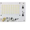
Светодиодное освещение в сборе с печатной платы большого объема
Название: Светодиодное освещение в сборе печатной платы большого объема
Происхождение: Китай
Сертифицировано: UL, CE, RoHS.
Базовый материал: FR-4/алюминий/керамика/cem-3/FR-1
Паяльная маска: Белый Черный Зеленый Синий Красный
Применение: Светодиодное освещение
Поверхностная обработка: HASL\OSP\погружное золото
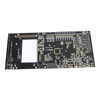
Сборка печатной платы большого объема для игровой консоли
Название: Сборка печатной платы большого объема для игровой консоли
Происхождение: Китай
Сертифицировано: UL, CE, RoHS.
Слои: 1л
Базовый материал: FR-4
Толщина платы: по индивидуальному заказу
Толщина меди: 1 унция
Поверхностная обработка: бессвинцовый HASL
Применение: для игр
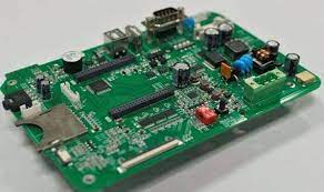
Компьютерная материнская плата в сборе
Название: Компьютерная материнская плата в сборе
Происхождение: Китай
Сертифицировано: UL, CE, RoHS.
Толщина меди: 1/3 унции – 4 унции o
Материал: ФР4
Поверхностная обработка: HASL\OSP\погружное золото
приложения: для компьютерных устройств
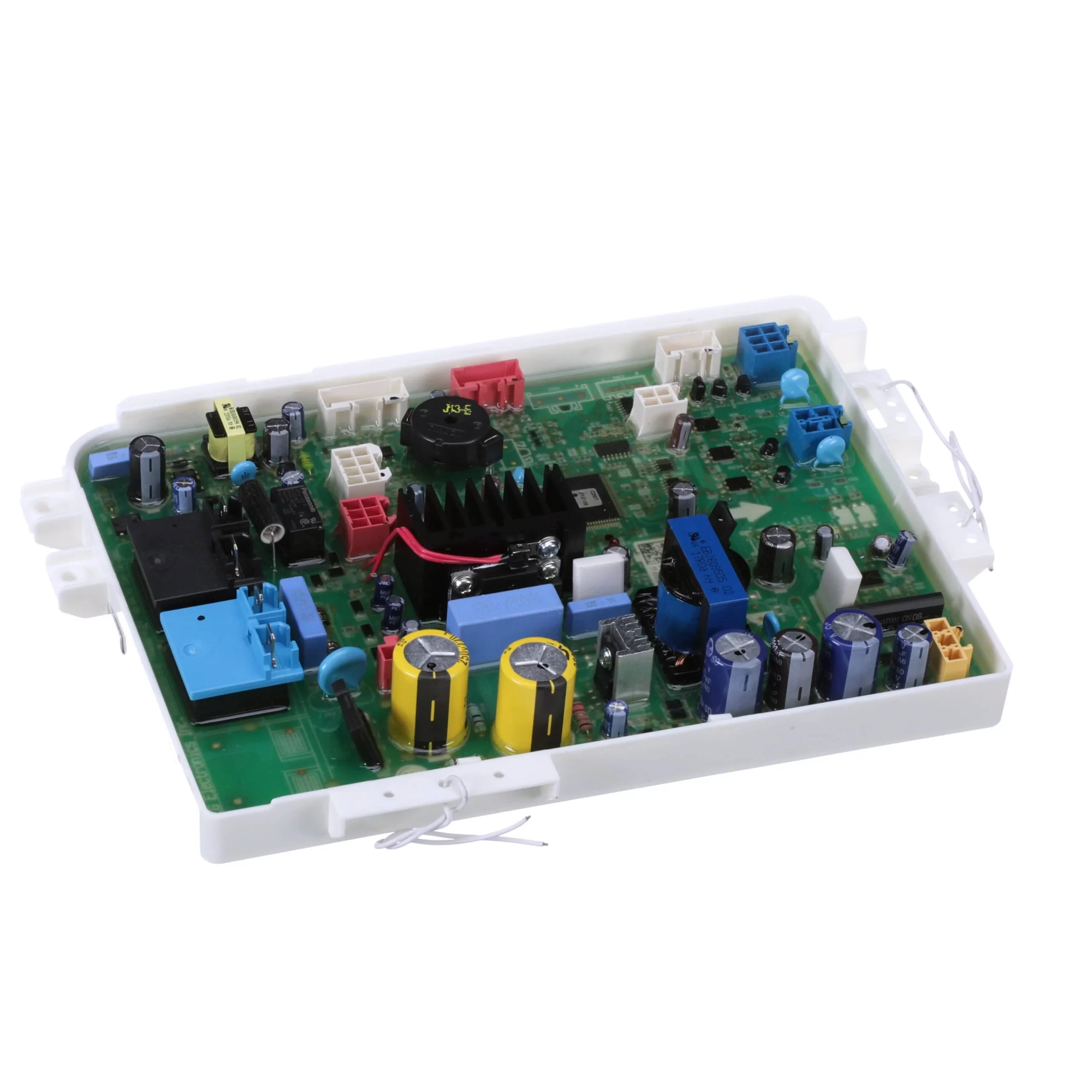
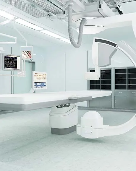
Главный блок управления посудомоечной машины
Название: Главный блок управления посудомоечной машины.
Происхождение: Китай
Сертифицировано: UL, CE, RoHS.
Толщина платы: по индивидуальному заказу
Поверхностная обработка: HASL/бессвинцовый HASL
Паяльная маска: зеленая, синяя, белая, красная и т. д.
Материнская плата телевизора в сборе
Название: Материнская плата телевизора в сборе с печатной платой большого объема
Происхождение: Китай
Сертифицировано: UL, CE, RoHS.
Поверхностная обработка: HASL\OSP\погружное золото
Толщина меди: 1-5 унций
приложения: электронный продукт
Толщина платы: по индивидуальному заказу
Материнская плата для смартфонов PCB плата большого объема
Название: Материнская плата для смартфонов, плата большого объема
Происхождение: Китай
Сертифицировано: UL, CE, RoHS.
Цвет паяльного резиста: Зеленый; Красный; Желтый; Черный; Белый
Материал: FR4 CEM1 CEM3 Высота TG
Применение: Электронный продукт
Толщина платы: по индивидуальному заказу
- PCB Assembly Capability
- PCB Assembly Equipment
High Volume PCB Assembly is a specialized electronic manufacturing service designed to meet the demands of large-scale production. It involves the efficient and rapid assembly of printed circuit boards (PCBs) in high quantities to meet the requirements of industries. It includes consumer electronics, automotive, also telecommunications, and more.
High Volume PCB utilizes advanced automated assembly processes, state-of-the-art equipment, and streamlined production workflows to ensure the fast and accurate assembly of PCBs. It also involves the mounting of various electronic components onto the PCB. This includes integrated circuits (ICs), resistors, capacitors, connectors, and more.
Advantages of High-Volume PCB Assembly:
- Efficient Production: High Volume Assembly is specifically designed for efficient production in large quantities. The utilization of automated pick-and-place machines, soldering equipment, and inspection systems allows for rapid assembly. It also reduces manufacturing lead times and increases production throughput.
- Consistency and Quality Control: High Volume Assembly employs robust quality control measures to ensure consistency and reliability in the assembled PCBs. Automated inspection systems perform checks for component placement accuracy, solder joint quality, and other critical parameters. This also enables high-quality standards are met consistently across the production run.
- Cost-Effectiveness: With its optimized production processes and economies of scale, High Volume PCB Assembly offers cost-effective solutions for large-scale production. The automated assembly processes minimize labor costs, while efficient material management reduces waste and lowers overall production expenses.
- Scalability: High Volume PCB is highly scalable, making it suitable for both medium and large production runs. The streamlined processes and automated equipment allow for seamless scalability. This ensures that the production capacity can be adjusted to meet changing market demands.
- Design for Manufacturability (DFM): DFM principles are incorporated into the High Volume Assembly process to optimize the manufacturability of the PCB design. Design considerations such as component placement, PCB layout, and assembly constraints are evaluated to enhance the efficiency and quality of the assembly process.
| SMT capacity: 19 million points/day | ||
| Testing Equipment | X-RAY Nondestructive Tester, First Piece Tester, AOI Automatic Optical Tester, ICT Tester, BGA Rework Station | |
| Placement speed | Chip placement speed (at best conditions) 0.036 S/piece | |
| Mounted Component Specifications | Pasteable smallest package | |
| Minimum device accuracy | ||
| IC type chip accuracy | ||
| Mounted PCB Specifications | Substrate size | |
| Substrate thickness | ||
| throw rate | 1. Resistance-capacitance ratio 0.3% | |
| 2. IC type without throwing material | ||
| Board Type | POP/common board/FPC/rigid-flex board/metal substrate | |
| DIP daily production capacity | ||
| DIP plug-in production line | 50000 points/day | |
| DIP post welding production line | 20000 points/day | |
| DIP test production line | 50000pcs PCBA/day | |
| Assembly processing capability | ||
| The company has more than 10 advanced assembly production lines, dust-free and anti-static air-conditioning workshop, TP dust-free workshop, equipped with aging room, test room, functional test isolation room, advanced and perfect equipment, can carry out various product assembly, packaging, testing, Aging, etc. production. Monthly production capacity can reach 150,000 to 300,000 sets/month | ||
| PCBA processing capability | ||
| project | Mass processing capability | Small batch processing capability |
| Number of layers (max) | 2-18 | 20-30 |
| Plate type | FR-4, Ceramic Sheet, Aluminum Base Sheet PTFE, Halogen Free Sheet, High Tg Sheet | PTFE, PPO, PPE |
| Rogers,etc Teflon | E-65, ect | |
| Sheet mixing | 4 layers – 6 layers | 6th floor – 8th floor |
| biggest size | 610mm X 1100mm | / |
| Dimensional Accuracy | ±0.13mm | ±0.10mm |
| Plate thickness range | 0.2mm–6.00mm | 0.2mm–8.00mm |
| Thickness tolerance ( t≥0.8mm) | ±8% | ±5% |
| Thickness tolerance (t<0.8mm) | ±10% | ±8% |
| Media thickness | 0.076mm–6.00mm | 0.076mm–0.100mm |
| Minimum line width | 0.10mm | 0.075mm |
| Minimum spacing | 0.10mm | 0.075mm |
| Outer copper thickness | 8.75um–175um | 8.75um–280um |
| Inner layer copper thickness | 17.5um–175um | 0.15mm–0.25mm |
| Drilling hole diameter (mechanical drill) | 0.25mm–6.00mm | 0.15mm–0.25mm |
| Hole diameter (mechanical drill) | 0.20mm–6.00mm | 0.10mm–0.20mm |
| Hole Tolerance (Mechanical Drill) | 0.05mm | / |
| Hole tolerance (mechanical drill) | 0.075mm | 0.050mm |
| Laser Drilling Aperture | 0.10mm | 0.075mm |
| Plate thickness aperture ratio | 10:1 | 12:1 |
| Solder mask type | Photosensitive green, yellow, black, purple, blue, ink | / |
| Minimum Solder Mask Bridge Width | 0.10mm | 0.075mm |
| Minimum Solder Mask Isolation Ring | 0.05mm | 0.025mm |
| Plug hole diameter | 0.25mm–0.60mm | 0.60mm-0.80mm |
| Impedance tolerance | ±10% | ±5% |
| Surface treatment type | Hot air leveling, chemical nickel gold, immersion silver, electroplated nickel gold, chemical immersion tin, gold finger card board | Immersion Tin, OSP |

Automatic Solder Paste Printing Machine

AOI Optical Inspection

Smt High-Speed Placement Machine

Nitrogen Reflow Soldering

X-Ray

Three Anti-Paint Spraying Machine

SPI Solder Paste Thickness Tester

Automatic Wave Soldering Machine

First Article Inspection
Our complete turnkey PCB assembly service provides a 24 hour quote service for your turnkey PCB assembly order.
LEIYAO cooperates with world-renowned component suppliers to ensure that the source of electronic components is plastic and the authenticity is guaranteed.
It has 7 fully automatic SMT high-speed chip production lines, equipped with ten temperature zone nitrogen reflow ovens, online AOI, SPI, X-RAY and other equipment.
We have complete ISO9001, ISO13485, ISO14001, IATF 16949, UL and other system certifications, and our products meet environmental protection requirements.