Производитель подключаемых модулей DIP – SMT Patch
Название: Производитель подключаемых модулей DIP — SMT Patch
Происхождение: Китай
Сертифицировано: UL, CE, RoSH.
Толщина платы: 1,6 мм
Толщина меди: 1 унция
Паяльная маска: Белый
Отделка поверхности
бессвинцовый хасл, OSP, Immersion Gold, иммерсионная банка

PCB Textolite SMT плата приемника дронов
Название: PCB Textolite SMT, плата приемника дронов
Происхождение: Китай
Сертифицировано: UL, CE, RoSH.
Толщина платы: 1,0-1,6 мм
Толщина меди: 1 унция, 1-12 унций
Поверхностная обработка: OSP/HASL/погружное золото
Количество слоев: 1-16 слоев

DIP-модуль для обработки медицинских устройств
Название: Подключаемый модуль DIP для обработки медицинских устройств
Происхождение: Китай
Сертифицировано: UL, CE, RoHS.
Применение: Электронное устройство
Слой: 2 слоя
Толщина платы: по индивидуальному заказу
Толщина меди: 1 унция

Сборка электронных компонентов для обработки печатных плат и SMT DIP
Название: PCB и сборка электронных компонентов для обработки плагина DIP SMT
Происхождение: Китай
Сертифицировано: UL, CE, RoHS.
Отделка поверхности: бессвинцовый хасл
Толщина меди: 3 унции
Материал: ФР4
Толщина платы: по индивидуальному заказу
Паяльная маска: Белый
- PCB Assembly Capability
- PCB Assembly Equipment
- PCB Assembly Capability
The DIP (Dual In-Line Package) plug-in processing solution is a versatile and efficient method for integrating electronic components onto printed circuit boards (PCBs). This plug-in processing technique allows for easy insertion and removal of components into DIP sockets on the PCB, offering a flexible and modular approach to electronic assembly.
The DIP plug-in processing solution involves the use of DIP packages, which consist of individual electronic components encapsulated in rectangular-shaped housings with two parallel rows of pins. These pins are designed to fit into corresponding sockets on the PCB, creating a reliable and secure electrical connection.
With DIP electronic components such as integrated circuits (ICs), resistors, capacitors, and other discrete devices can be conveniently mounted onto the PCB without the need for complex soldering processes. Instead, the components are inserted into the DIP sockets, allowing for easy replacement or reconfiguration as needed.
Advantages of DIP Plug-in Processing:
- Versatility and Modularity: DIP processing provides a high level of versatility and modularity in electronic assembly. Components can be easily plugged in or removed from DIP sockets, facilitating rapid prototyping, testing, and system modifications. This flexibility also allows for efficient design iterations and simplifies maintenance and repairs.
- Time and Cost Efficiency: The plug-in nature of DIP processing significantly reduces the time and cost associated with assembly and rework. The absence of soldering eliminates the need for specialized soldering equipment, reducing setup and labor costs. Additionally, the ability to quickly replace faulty components improves repair turnaround time and minimizes downtime.
- Accessibility for Testing and Debugging: DIP processing provides easy access to components for testing and debugging purposes. During the development phase, engineers can quickly insert or remove components to assess their functionality and troubleshoot any issues. This accessibility aids in the efficient identification and resolution of problems, reducing development cycles.
- Component Compatibility and Interchangeability: DIP packages offer broad compatibility with various electronic components. The standardized pin configurations and socket layouts ensure compatibility across a wide range of ICs and discrete devices. This interchangeability simplifies component sourcing, inventory management, and system upgrades.
- High Connection Reliability: DIP sockets provide reliable electrical connections between components and PCBs. The pins and sockets are designed to create secure contacts, ensuring consistent and robust signal transmission. This reliability is crucial for maintaining signal integrity and also minimizing the risk of loose connections or intermittent faults.
| Item | Process Capability Parameter |
| Order Quantity | ≥1PC |
| Quality Grade | IPC-A-610 |
| Lead Time | 24 hours expedited service can be offered. 3- 4 days normally for PCBA prototype orders. We will give you an accurate lead time when we quote for you. |
| Size | 50*50mm~510*460mm |
| Board Type | Rigid PCB, Flexible PCB, metal core PCB |
| Min Package | 01005 (0.4mm*0.2mm) |
| Max Package | No limit |
| Mounting Accuracy | ±0.035mm(±0.025mm) Cpk≥1.0 (3σ) |
| Surface Finish | Lead/Lead-free HASL, Immersion gold, OPS, etc. |
| Assembly Types | Surface mount (SMT), Through-hole (DIP), Mixed Technology (SMT & Thru-hole) |
| Component Sourcing | Turnkey (All components sourced by PCBMay), Partial turnkey, Kitted/Consigned |
| BGA Package | BGA Dia. 0.14mm, BGA 0.2mm pitch |
| SMT Parts Presentation | Cut Tape, Partial reel, Reel,Tube, Tray, Laser-cut Stainless Steel |
| Cable Assembly | We supply custom cables, cable assemblies, wiring looms/harnesses and power leads for various industries including automotive, security, mining, medical and entertainment. |
| Stencil | Stencil with or without frame (offered free by PCBMay) |
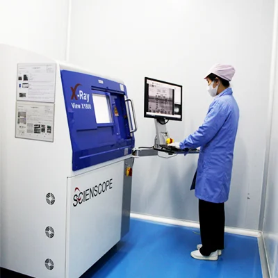
| Quality Inspection | Visual inspection; AOI checking; BGA placement – X-RAY checking |
| SMT Capacity | 3 Million~4 Million Soldering Pad/day |
| DIP Capacity | 100 Thousand Pins/day |
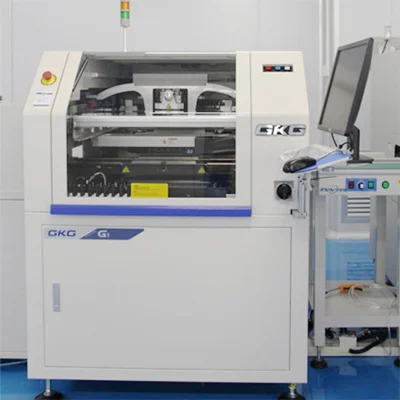
Automatic Solder Paste Printing Machine
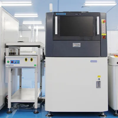
AOI Optical Inspection
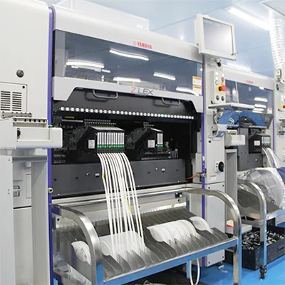
Smt High-Speed Placement Machine
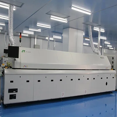
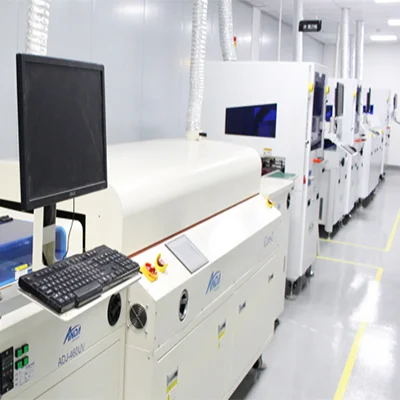
Nitrogen Reflow Soldering
X-Ray
Three Anti-Paint Spraying Machine
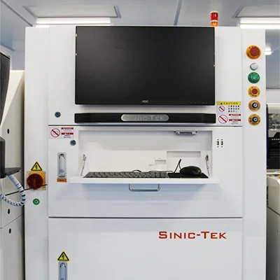
SPI Solder Paste Thickness Tester
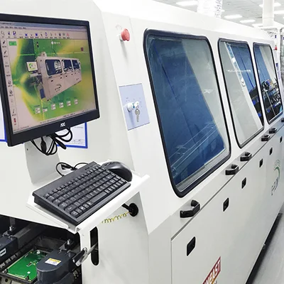
Automatic Wave Soldering Machine
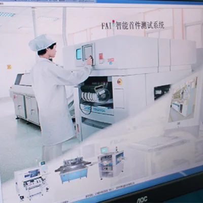
First Article Inspection
| SMT capacity: 19 million points/day | ||
| Testing Equipment | X-RAY Nondestructive Tester, First Piece Tester, AOI Automatic Optical Tester, ICT Tester, BGA Rework Station | |
| Placement speed | Chip placement speed (at best conditions) 0.036 S/piece | |
| Mounted Component Specifications | Pasteable smallest package | |
| Minimum device accuracy | ||
| IC type chip accuracy | ||
| Mounted PCB Specifications | Substrate size | |
| Substrate thickness | ||
| throw rate | 1. Resistance-capacitance ratio 0.3% | |
| 2. IC type without throwing material | ||
| Board Type | POP/common board/FPC/rigid-flex board/metal substrate | |
| DIP daily production capacity | ||
| DIP plug-in production line | 50000 points/day | |
| DIP post welding production line | 20000 points/day | |
| DIP test production line | 50000pcs PCBA/day | |
| Assembly processing capability | ||
| The company has more than 10 advanced assembly production lines, dust-free and anti-static air-conditioning workshop, TP dust-free workshop, equipped with aging room, test room, functional test isolation room, advanced and perfect equipment, can carry out various product assembly, packaging, testing, Aging, etc. production. Monthly production capacity can reach 150,000 to 300,000 sets/month | ||
| PCBA processing capability | ||
| project | Mass processing capability | Small batch processing capability |
| Number of layers (max) | 2-18 | 20-30 |
| Plate type | FR-4, Ceramic Sheet, Aluminum Base Sheet PTFE, Halogen Free Sheet, High Tg Sheet | PTFE, PPO, PPE |
| Rogers,etc Teflon | E-65, ect | |
| Sheet mixing | 4 layers – 6 layers | 6th floor – 8th floor |
| biggest size | 610mm X 1100mm | / |
| Dimensional Accuracy | ±0.13mm | ±0.10mm |
| Plate thickness range | 0.2mm–6.00mm | 0.2mm–8.00mm |
| Thickness tolerance ( t≥0.8mm) | ±8% | ±5% |
| Thickness tolerance (t<0.8mm) | ±10% | ±8% |
| Media thickness | 0.076mm–6.00mm | 0.076mm–0.100mm |
| Minimum line width | 0.10mm | 0.075mm |
| Minimum spacing | 0.10mm | 0.075mm |
| Outer copper thickness | 8.75um–175um | 8.75um–280um |
| Inner layer copper thickness | 17.5um–175um | 0.15mm–0.25mm |
| Drilling hole diameter (mechanical drill) | 0.25mm–6.00mm | 0.15mm–0.25mm |
| Hole diameter (mechanical drill) | 0.20mm–6.00mm | 0.10mm–0.20mm |
| Hole Tolerance (Mechanical Drill) | 0.05mm | / |
| Hole tolerance (mechanical drill) | 0.075mm | 0.050mm |
| Laser Drilling Aperture | 0.10mm | 0.075mm |
| Plate thickness aperture ratio | 10:1 | 12:1 |
| Solder mask type | Photosensitive green, yellow, black, purple, blue, ink | / |
| Minimum Solder Mask Bridge Width | 0.10mm | 0.075mm |
| Minimum Solder Mask Isolation Ring | 0.05mm | 0.025mm |
| Plug hole diameter | 0.25mm–0.60mm | 0.60mm-0.80mm |
| Impedance tolerance | ±10% | ±5% |
| Surface treatment type | Hot air leveling, chemical nickel gold, immersion silver, electroplated nickel gold, chemical immersion tin, gold finger card board | Immersion Tin, OSP |


