
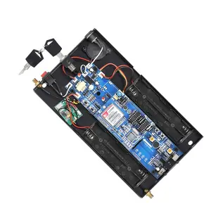
Автоматическая система разблокировки дверных замков в сборе с печатной платой
Название: Автоматическая система разблокировки дверных замков в сборе с печатной платой
Происхождение: Китай
Сертифицировано: UL, CE, RoHS.
Поверхностная обработка: ENIG/HASL/погружное олово/погружное серебро/твердое золото
Паяльная маска: зеленая, синяя, белая, красная и т. д.
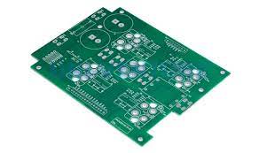
Бытовая автомобильная электронная печатная плата в сборе
Название: Печатная плата для бытовой автомобильной электроники
Происхождение: Китай
Сертифицировано: UL, CE, RoHS.
Толщина меди: 1 унция
Толщина платы: по индивидуальному заказу
Поверхностная обработка: ОСП
Паяльная маска: Белый

Сборка печатных плат для бытовой аэрокосмической электронной техники
Название: Сборка печатных плат для бытовой аэрокосмической электронной промышленности
Происхождение: Китай
Сертифицировано: UL, CE, RoHS.
Материал: FR4, CEM1, CEM3, высокочастотная плата,
Форма: Прямоугольная, Круглая, Прорези, Вырезы, Сложная, Неправильная
Поверхностная обработка: HASL, ENIG, OSP и т. д.
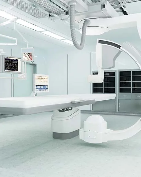
Сборка печатных плат для медицинских устройств
Название: Сборка печатных плат для медицинских устройств
Происхождение: Китай
Сертифицировано: UL, CE, RoHS.
Базовый материал: FR4, FR4 CEM1 CEM3 Высота TG
Поверхностная обработка: OSP, ENIG, HASL
Цвет паяльной маски: черный, белый, желтый
Толщина меди: 0,5 унции ~ 5 унций

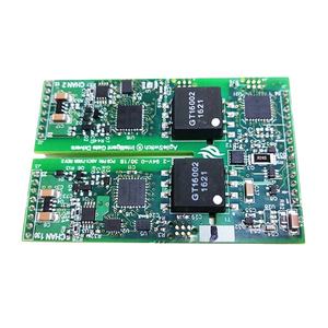
Производитель печатных плат бытовой электроники в Китае
Название: Производитель печатных плат бытовой электроники в Китае
Происхождение: Китай
Сертифицировано: UL, CE, RoHS.
Паяльная маска: зеленая, красная, белая, черная, желтая,
Поверхностная обработка:
OSP,HASL-LF, ENIG, Им-Ан, Им-Аг
Применение: Электронные продукты
Материал: FR-4, CEM, TG170, без галогенов, по индивидуальному заказу.
- PCB Assembly Capability
- PCB Assembly Equipment
Our Consumer Electronics PCBA (Printed Circuit Board Assembly) service caters specifically to the assembly and manufacturing needs of consumer electronic devices. From smartphones and tablets to gaming consoles and smart home devices, our experienced team and state-of-the-art facilities ensure the highest quality and performance of your consumer electronic products.
We specialize in the assembly of complex PCBs with a wide range of components, including microprocessors, memory modules, sensors, connectors, and more. Our advanced assembly techniques and stringent quality control measures guarantee precise component placement, secure soldering, and also optimal functionality.
Advantages of Consumer Electronics PCBA:
- Expertise in consumer electronics: Our team possesses extensive experience in the assembly of consumer electronics, understanding the unique requirements and challenges of this industry. We stay up-to-date with the latest technological advancements. This also ensures that your products meet the highest industry standards.
- Customized solutions: We offer flexible and customized PCBA solutions tailored to your specific consumer electronic product requirements. Whether you need a high-volume production run or a smaller batch, we can accommodate your needs while maintaining consistency and also quality.
- Quality assurance: Quality is paramount in consumer electronics, and we prioritize it throughout the assembly process. Our stringent quality control procedures. This also includes thorough testing and inspection, guarantee that your products meet the highest standards of performance, reliability, and safety.
- Cost-effective manufacturing: We understand the competitive nature of the consumer electronics market. Our optimized manufacturing processes, efficient supply chain management, and economies of scale allow us to provide cost-effective PCBA services without compromising on quality.
- Timely delivery: We recognize the importance of meeting deadlines in the fast-paced consumer electronics industry. Our streamlined production processes and project management ensure timely delivery of your PCBA orders. This also enables you to stay ahead in the market.
| SMT capacity: 19 million points/day | ||
| Testing Equipment | X-RAY Nondestructive Tester, First Piece Tester, AOI Automatic Optical Tester, ICT Tester, BGA Rework Station | |
| Placement speed | Chip placement speed (at best conditions) 0.036 S/piece | |
| Mounted Component Specifications | Pasteable smallest package | |
| Minimum device accuracy | ||
| IC type chip accuracy | ||
| Mounted PCB Specifications | Substrate size | |
| Substrate thickness | ||
| throw rate | 1. Resistance-capacitance ratio 0.3% | |
| 2. IC type without throwing material | ||
| Board Type | POP/common board/FPC/rigid-flex board/metal substrate | |
| DIP daily production capacity | ||
| DIP plug-in production line | 50000 points/day | |
| DIP post welding production line | 20000 points/day | |
| DIP test production line | 50000pcs PCBA/day | |
| Assembly processing capability | ||
| The company has more than 10 advanced assembly production lines, dust-free and anti-static air-conditioning workshop, TP dust-free workshop, equipped with aging room, test room, functional test isolation room, advanced and perfect equipment, can carry out various product assembly, packaging, testing, Aging, etc. production. Monthly production capacity can reach 150,000 to 300,000 sets/month | ||
| PCBA processing capability | ||
| project | Mass processing capability | Small batch processing capability |
| Number of layers (max) | 2-18 | 20-30 |
| Plate type | FR-4, Ceramic Sheet, Aluminum Base Sheet PTFE, Halogen Free Sheet, High Tg Sheet | PTFE, PPO, PPE |
| Rogers,etc Teflon | E-65, ect | |
| Sheet mixing | 4 layers – 6 layers | 6th floor – 8th floor |
| biggest size | 610mm X 1100mm | / |
| Dimensional Accuracy | ±0.13mm | ±0.10mm |
| Plate thickness range | 0.2mm–6.00mm | 0.2mm–8.00mm |
| Thickness tolerance ( t≥0.8mm) | ±8% | ±5% |
| Thickness tolerance (t<0.8mm) | ±10% | ±8% |
| Media thickness | 0.076mm–6.00mm | 0.076mm–0.100mm |
| Minimum line width | 0.10mm | 0.075mm |
| Minimum spacing | 0.10mm | 0.075mm |
| Outer copper thickness | 8.75um–175um | 8.75um–280um |
| Inner layer copper thickness | 17.5um–175um | 0.15mm–0.25mm |
| Drilling hole diameter (mechanical drill) | 0.25mm–6.00mm | 0.15mm–0.25mm |
| Hole diameter (mechanical drill) | 0.20mm–6.00mm | 0.10mm–0.20mm |
| Hole Tolerance (Mechanical Drill) | 0.05mm | / |
| Hole tolerance (mechanical drill) | 0.075mm | 0.050mm |
| Laser Drilling Aperture | 0.10mm | 0.075mm |
| Plate thickness aperture ratio | 10:1 | 12:1 |
| Solder mask type | Photosensitive green, yellow, black, purple, blue, ink | / |
| Minimum Solder Mask Bridge Width | 0.10mm | 0.075mm |
| Minimum Solder Mask Isolation Ring | 0.05mm | 0.025mm |
| Plug hole diameter | 0.25mm–0.60mm | 0.60mm-0.80mm |
| Impedance tolerance | ±10% | ±5% |
| Surface treatment type | Hot air leveling, chemical nickel gold, immersion silver, electroplated nickel gold, chemical immersion tin, gold finger card board | Immersion Tin, OSP |

Automatic Solder Paste Printing Machine

AOI Optical Inspection

Smt High-Speed Placement Machine

Nitrogen Reflow Soldering

X-Ray

Three Anti-Paint Spraying Machine

SPI Solder Paste Thickness Tester

Automatic Wave Soldering Machine

First Article Inspection