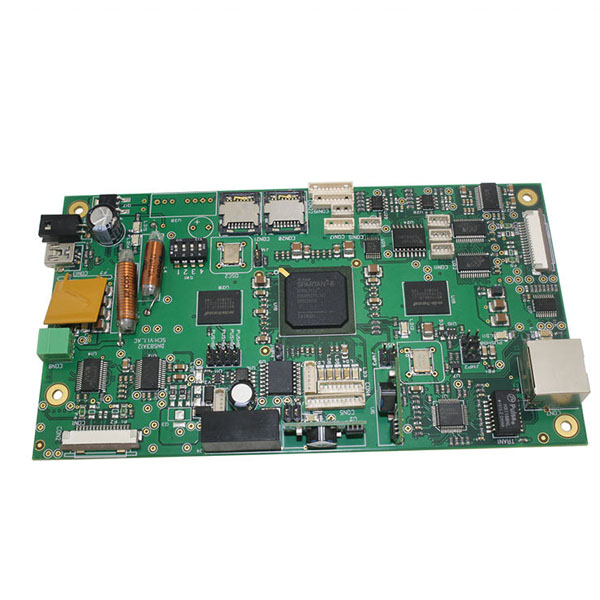
BGA PCB SMT Сборка электроники PCBA EMS Service
Количество слоев: 1,2,4 или 6, до 18 слоев.
Количество заказа: от 1 до 50 000
Форма платы:Прямоугольная,круглая,прорези,вырезы,сложная,неправильная
Тип доски:Жесткая, Гибкая, Жестко-гибкая
Материал платы: стеклоэпоксидная смола FR-4, высокая Tg FR-4, соответствует требованиям Rohs, алюминий, Rogers и т. д.
Резка плат: сдвиг, V-образный вырез, маршрутизация с выступами
Толщина платы: 0,2-4,0 мм, гибкость 0,01-0,25 мм
Вес меди: 1,0, 1,5, 2,0 унции
Паяльная маска: двусторонняя зеленая LPI, также поддерживает красный, белый, желтый, синий, черный
Шелкография: двусторонняя или односторонняя белого, желтого, черного или негативного цвета.
Минимальная ширина линии шелкографии: 0,006 дюйма или 0,15 мм.
Максимальные размеры платы: 20 дюймов * 20 дюймов или 500 мм * 500 мм.
Минимальный след/зазор: 0,10 мм или 4 мила
Минимальный диаметр сверла: 0,01 дюйма, 0,25 мм или 10 мил
Поверхностная обработка: HASL, никель, иммерсионное золото, иммерсионное олово, иммерсионное серебро, OSP и т. д.
Допуск толщины платы: ± 10%
Допуск на вес меди: ± 0,25 унции
Минимальная ширина паза: 0,12 дюйма, 3,0 мм или 120 мил.
Глубина V-Score: 20–25 % толщины доски.
Формат файла проекта: Gerber RS-274,274D, Eagle и AutoCAD DXF, DWG.
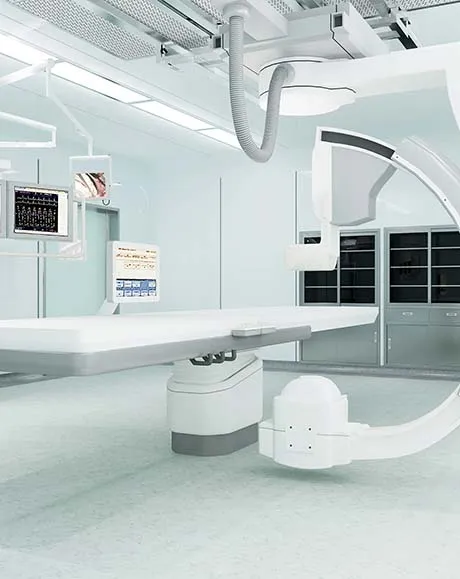
Платы для пульсоксиметра, комплексное обслуживание PCBA
Название продукта: Служба сборки печатных плат
Тип: Жесткий
Материал: FR4, CEM1, CEM3, высокочастотная плата, Роджерс
Слой: 1,2,4,6…20Слой
Форма: Прямоугольная, Круглая, Прорези, Вырезы, Сложная, Неправильная
Режущий сдвиг, V-образный вырез, фрезерование с выступами
Толщина платы 0,2-4 мм, обычная 1,6 мм.
Толщина меди: 0,5-4 унции, обычная 1 унция
Паяльная маска: зеленая, красная, синяя, желтая и т. д.
Шелкография: белый, черный и т. д.
Минимальная ширина линии шелкографии: 0,006 дюйма или 0,15 мм.
Минимальный след/зазор: 0,1 мм или 4 мила
Минимальный диаметр сверла 0,01 дюйма, 0,25 мм или 10 мил
Поверхностная обработка HASL, ENIG, OSP и т. д.
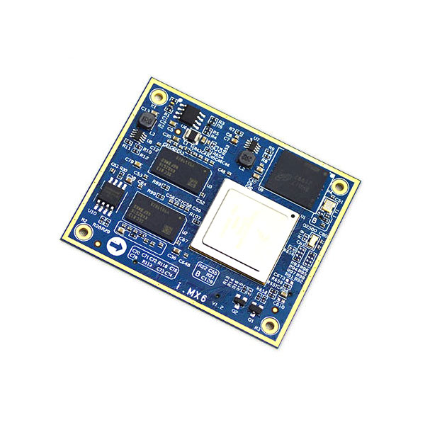
Модуль ARM Cortex A7 i.MX6 SOM
Имя: Сборка BGA
ЦП:: Четырехъядерный процессор ARM Cortex A53 1,28-1,5 ГГц, MT6739
Операционная система: Android 7.0、8.1
Основная информация: GSM 850/900/1800/1900.
Экран: высочайшая поддержка HD+ (1440*720), интерфейс MIPI.
Размер модуля: 55,5*38,5*3 мм
Номер контакта: 146pin
Слои: 10 слоев ENIG
Вспышка: 1+8, 2+16, 3+32.
Wi-Fi: IEEE 802.11 b/g/n, двухдиапазонный 2,4 ГГц/5 ГГц
GPS: поддержка GPS/ГЛОНАСС AGPS
Bluetooth: BT 4,0, 3,0, 2,1, поддержка BLE
- PCB Assembly Capability
- PCB Assembly Equipment
Introducing BGA (Ball Grid Array) Assembly services, the cutting-edge solution for precise and reliable assembly of complex electronic components. BGA Assembly involves the mounting and soldering of Ball Grid Array packages onto printed circuit boards, providing high-density interconnectivity and enhanced performance for advanced electronic systems.
At our advanced facility, we offer comprehensive BGA Assembly services to meet the demanding requirements of modern electronics. Our state-of-the-art equipment and skilled technicians ensure accurate placement, precise soldering, and meticulous quality control throughout the assembly process.
BGA Assembly is known for its ability to accommodate densely packed components, resulting in compact and efficient circuit designs. By utilizing an array of solder balls instead of traditional leads, BGA packages offer improved electrical performance, reduced signal noise, and enhanced thermal dissipation.
We specialize in handling various BGA types, including micro BGAs, fine-pitch BGAs, and large-scale BGAs, to cater to diverse application needs. Whether it’s consumer electronics, telecommunications, medical devices, or aerospace systems, our BGA services deliver precise and high-performance assemblies.
Advantages of BGA Assembly:
- High-Density Interconnectivity: BGA allows for densely packed components, enabling compact circuit designs and efficient use of PCB space.
- Enhanced Electrical Performance: BGA packages also offer improved electrical performance with reduced signal noise, shorter signal paths, and better impedance control.
- Efficient Thermal Dissipation: The ball grid array configuration facilitates efficient heat dissipation, preventing overheating and also ensuring reliable operation of high-power components.
- Reliable Soldering Connections: BGA employs advanced techniques like reflow soldering and underfill encapsulation to ensure strong and reliable solder joints.
- Meticulous Quality Control: We conduct thorough inspection procedures, including X-ray inspection and also thermal profiling, to verify proper solder joint formation and ensure assembly integrity.
| SMT capacity: 19 million points/day | ||
| Testing Equipment | X-RAY Nondestructive Tester, First Piece Tester, AOI Automatic Optical Tester, ICT Tester, BGA Rework Station | |
| Placement speed | Chip placement speed (at best conditions) 0.036 S/piece | |
| Mounted Component Specifications | Pasteable smallest package | |
| Minimum device accuracy | ||
| IC type chip accuracy | ||
| Mounted PCB Specifications | Substrate size | |
| Substrate thickness | ||
| throw rate | 1. Resistance-capacitance ratio 0.3% | |
| 2. IC type without throwing material | ||
| Board Type | POP/common board/FPC/rigid-flex board/metal substrate | |
| DIP daily production capacity | ||
| DIP plug-in production line | 50000 points/day | |
| DIP post welding production line | 20000 points/day | |
| DIP test production line | 50000pcs PCBA/day | |
| Assembly processing capability | ||
| The company has more than 10 advanced assembly production lines, dust-free and anti-static air-conditioning workshop, TP dust-free workshop, equipped with aging room, test room, functional test isolation room, advanced and perfect equipment, can carry out various product assembly, packaging, testing, Aging, etc. production. Monthly production capacity can reach 150,000 to 300,000 sets/month | ||
| PCBA processing capability | ||
| project | Mass processing capability | Small batch processing capability |
| Number of layers (max) | 2-18 | 20-30 |
| Plate type | FR-4, Ceramic Sheet, Aluminum Base Sheet PTFE, Halogen Free Sheet, High Tg Sheet | PTFE, PPO, PPE |
| Rogers,etc Teflon | E-65, ect | |
| Sheet mixing | 4 layers – 6 layers | 6th floor – 8th floor |
| biggest size | 610mm X 1100mm | / |
| Dimensional Accuracy | ±0.13mm | ±0.10mm |
| Plate thickness range | 0.2mm–6.00mm | 0.2mm–8.00mm |
| Thickness tolerance ( t≥0.8mm) | ±8% | ±5% |
| Thickness tolerance (t<0.8mm) | ±10% | ±8% |
| Media thickness | 0.076mm–6.00mm | 0.076mm–0.100mm |
| Minimum line width | 0.10mm | 0.075mm |
| Minimum spacing | 0.10mm | 0.075mm |
| Outer copper thickness | 8.75um–175um | 8.75um–280um |
| Inner layer copper thickness | 17.5um–175um | 0.15mm–0.25mm |
| Drilling hole diameter (mechanical drill) | 0.25mm–6.00mm | 0.15mm–0.25mm |
| Hole diameter (mechanical drill) | 0.20mm–6.00mm | 0.10mm–0.20mm |
| Hole Tolerance (Mechanical Drill) | 0.05mm | / |
| Hole tolerance (mechanical drill) | 0.075mm | 0.050mm |
| Laser Drilling Aperture | 0.10mm | 0.075mm |
| Plate thickness aperture ratio | 10:1 | 12:1 |
| Solder mask type | Photosensitive green, yellow, black, purple, blue, ink | / |
| Minimum Solder Mask Bridge Width | 0.10mm | 0.075mm |
| Minimum Solder Mask Isolation Ring | 0.05mm | 0.025mm |
| Plug hole diameter | 0.25mm–0.60mm | 0.60mm-0.80mm |
| Impedance tolerance | ±10% | ±5% |
| Surface treatment type | Hot air leveling, chemical nickel gold, immersion silver, electroplated nickel gold, chemical immersion tin, gold finger card board | Immersion Tin, OSP |

Automatic Solder Paste Printing Machine

AOI Optical Inspection

Smt High-Speed Placement Machine

Nitrogen Reflow Soldering

X-Ray

Three Anti-Paint Spraying Machine

SPI Solder Paste Thickness Tester

Automatic Wave Soldering Machine

First Article Inspection
Our complete turnkey PCB assembly service provides a 24 hour quote service for your turnkey PCB assembly order.
Leadsintec cooperates with world-renowned component suppliers to ensure that the source of electronic components is plastic and the authenticity is guaranteed.
It has 7 fully automatic SMT high-speed chip production lines, equipped with ten temperature zone nitrogen reflow ovens, online AOI, SPI, X-RAY and other equipment.
We have complete ISO9001, ISO13485, ISO14001, IATF 16949, UL and other system certifications, and our products meet environmental protection requirements.